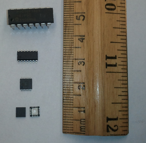
The same chip is often produced in several different packages. Here is an example: Microchip’s PIC16F1825 microcontroller, which is available in four different standard packages. The best package for your application depends on several factors. In many cases, it’s a tradeoff of size vs. ease of manufacturing.
For hobbyists, DIP (Dual In-Line) form factor, also known as a “through-hole” component, is the easiest to work with. DIP parts (the top chip above is an example) can be used in circuit boards, placed in sockets, or used with solderless breadboards for quick prototyping of new circuits. They’re often quite a bit larger than other packages, though, so they’re not always the best choice for a manufactured product. Mounting DIP parts also requires holes to be drilled in the circuit board — an additional step which can add manufacturing expense.
The second chip from the top is the same 16F1825 microcontroller in SOIC (Small-Outline Integrated Circuit) packaging. SOIC chips are usually smaller than their DIP counterparts, and the leads are closer together. This allows them to take up less space on a circuit board, helping with device miniaturization. In addition, they (and the smaller types) are “surface-mount” (or SMT) components, meaning they do not require any holes to be drilled in the circuit board. They can be trickier to solder to than DIP parts, though, since the leads are closer together. You need a good soldering iron, thin solder, and good technique to solder these correctly.
The third chip from the top is the same 16F1825 microcontroller in TSSOP (Thin-Shrink Small Outline Package) form. It is similar to the SOIC form factor, but with much smaller lead-to-lead spacing. TSSOP parts are probably best handled with solder paste and a reflow oven.
Finally, the two chips at the bottom are in QFN (Quad Flat No-Leads) packaging. QFN-16 is the smallest standard size; for 14-pin parts like the 16F1825, this means that two of the pins are unused. (Two QFN chips are shown; the one on the right is upside-down to show the contacts on the bottom of the chip.) Since the contacts are on the bottom, solder paste and a reflow oven or hot-air rework station are required to work with QFN chips. These can save a lot of circuit board space (and therefore expense) in manufactured products, but can be very difficult to work with for hobbyists.
There are other popular chip packages available, notably “Quad Flat” packaging (QFP, LQFP, TQFP, etc); “Ball Grid Array” (BGA) packaging, and many others. These packages are mostly intended for use in manufacturing, though, although hobbyists continue to come up with novel ways to use them in homebrew devices.


