It’s always fun to learn of new processes and capabilities — especially when processes which used to be prohibitively expensive themselves benefit from new technologies such as CNC and 3D printing.
Since our department bought an LPKF PC board mill in 2010, we’ve had the in-house capability to produce what I call “1.5-layer” boards. Our mill can do the insulation passes on the top and bottom — and I have it dialed in well enough that the solder pads are viable on both sides and aligned. However, the process doesn’t plate vias. Any connections between the two sides of the board must rely on a manually-soldered lead through a hole. With complex designs involving dozens of vias, this adds not only hours of benchtop time but dozens of potential failure points to the board.
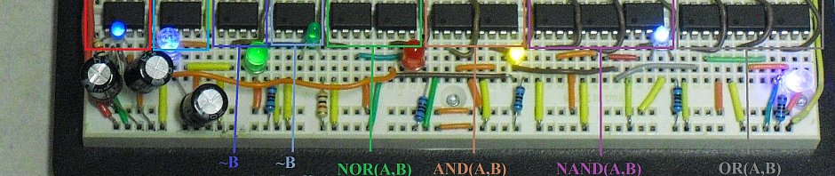
The existing solution has been, wherever possible, to keep all traces on the bottom side of the board, and use resistors and similar components as natural bridges across other traces. This has worked well for relatively simple boards like the TIL311 replacement hex decoder — but even this is pushing the style close to the reasonable limit. For more complex boards, 2- or 4-layer processes are needed.

(These were for a Mood Ring project for a local Girls, Inc. engineering activity.)
These days, provided you can wait a few days for the boards, there’s a better option. Modern PCB houses like PCBWay can accept your Gerber files over the ‘Net, apply a DRM check, and produce them with far more options than in-house production could provide. Even with shipping from China, you can have your boards in just a few days.
This capability has been available (for a steep price) for a number of years now — but recently, Just-In-Time manufacturing techniques and high levels of automation have meant that even small, custom orders can be turned around in a few days at surprisingly low cost.
Full disclosure: PCBWay kindly provided the boards ($41 value) for this Hex Decoder project free of charge in return for a writeup, but this review is my honest opinion — as is everything on this site.
With more students (and seemingly fewer remaining hex decoder boards) each year, I needed to make up some more hex decoders for next year’s Microprocessors class. PCBWay had recently contacted me, asking if I would be interested in reviewing their services, so I thought this would be the perfect opportunity. (Making boards with the LPKF is fun but time-consuming anyway, and there’s always the chance that something will go wrong and you’ll have to start the batch over. Maybe if I had an apprentice?)
So I packaged up the original FreePCB design into a semblance of normal-looking Gerber files, and uploaded it to PCBWay’s site. Somehow it passed the DFM checks, and within a few days (I may have submitted it on a Friday night right before Lunar New Year), a package with 20 boards was on its way to me.

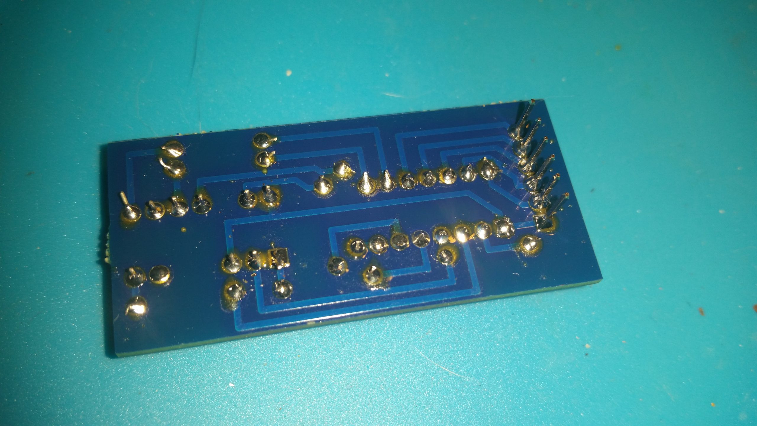
(Although the new process is capable of plated vias and reliable thin traces,
this design still reflects the original oversized, single-layer-or-bust style.)

The blue-on-blue text is a holdover from when this text was cut on the LPKF.
It was designed on the copper layer; I should have moved it to the silkscreen. Oops.
PCB design cognoscenti (of which I am not one!) will note that the pads are significantly larger (90 mil) than normal (50ish mil?), and the traces are quite large, too. This was because the original board was designed to be produced in-house using our PC board mill. This process produces untinned, hard-to-solder-to pads — and thin traces sometimes don’t survive the cutting process. Because of this, the DFM rules I used (25-50 mil traces, 90-mil pads on 100-mil spacings) could probably be met by a competent blacksmith.
PCBWay still manages to make it look pretty good, but I’m looking forward to designing boards with modern tolerances. No doubt fine-tuning the milling process would help, but outsourcing to a modern PC board house makes for much more reliable boards. So far, I’ve tried PCBWay as well as JLCPCB, and had very good results with both. PCBWay’s site seems a little easier to use, and they have some nice design sharing/selling features, and great customer support.
Once I found my old plans and got the necessary parts together, soldering was very easy; the plated pads and solder mask mean the solder goes where it should and not where it shouldn’t. Through-hole soldering is a piece of cake, and even SMD components — which are very experimental on the LPKF process — should be straightforward.
Everything worked great.
Bottom line: Even though PCBWay kindly comped the boards for this project, I’m impressed. These are decent, professional-quality boards with good tolerances, plated vias, solder masks, silkscreening, and more. They’re far better than we could make in-house, for something like a few dollars each — maybe even less, in quantity — and they can arrive in a week or two. If they’d only add yellow or gold silkscreen, we could even have them in school colors.
PCBWay isn’t the only good PC board house out there, but they provide good boards quickly at a nice low price, and have an easy-to-use site. Check them out.